
SPM測定サンプルデータ
USM1100
STM Topographic Image of Cinchonine molecules on Pt (100)
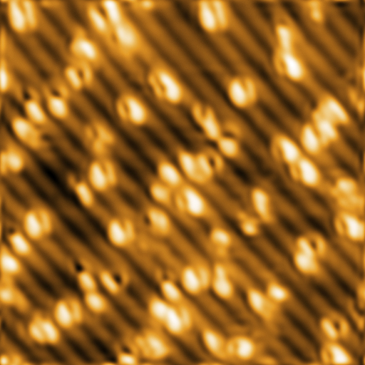
Temperature: Room Temperature
Field of View: 25nm × 25nm
Yutaka Miyatake
Unisoku Co., Ltd.
USM1200
STM Topographic Image of Si (100)

Temperature: 63K
Field of View: 3nm × 3nm
Dr. YOKOYAMA in Yokohama City Univ.
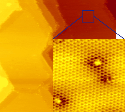
STM Molecular structure and Topographic Image of COOH-Porphyrin tetramer
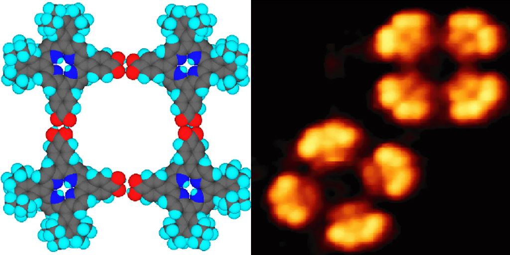
Temperature: 63K
Field of View: 11nm × 11nm
Dr. YOKOYAMA in Yokohama City Univ.
USM1300
STM Topographic Image of Si (111)
Temperature: 4.2K
Bias voltage: 0.84V
Tunnel current: 1.04nA
Field of veiw: 10nm × 10nm
Yutaka Miyatake
Unisoku Co., Ltd.
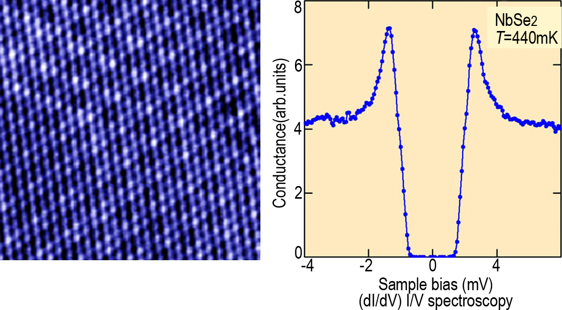
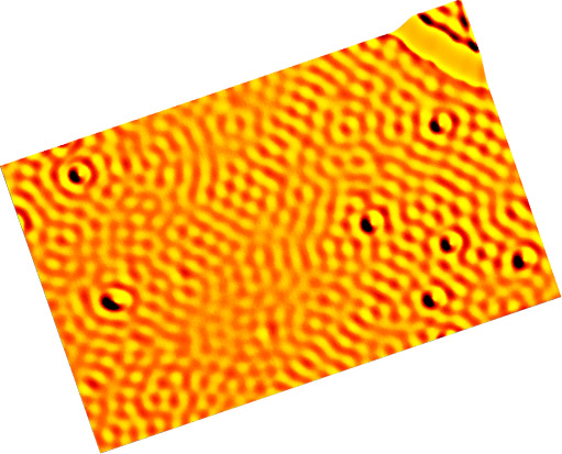
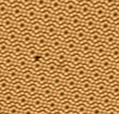
STM Topographic Image of vortex lattice of a superconductor NbSe2
Temperature: 400mK
Field: 0.5T
Environment: UHV
Field of View: 250nm × 250nm
Dr. HANAGURI
Magnetic Materials Laboratory, RIKEN
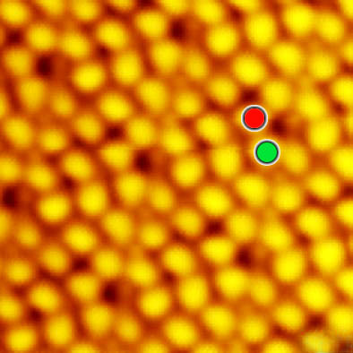
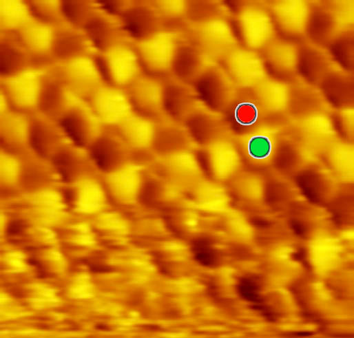
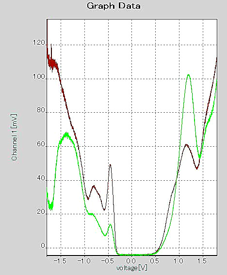
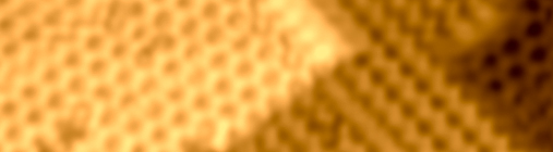
STM Topographic Image and STS data of Cleaved NBS2
Temperature: 440mK
Field of View: 7.3nm × 7.3nm
Dr. HANAGURI in Magnetic Materials Laboratory, RIKEN
Si (111) dI/dV topographic image in magnetic field (4.2K, 7t) by USM1300S 4He
Topo image
Sample bias 2.1V
Tunnel current 1.24nA
dI/dV image
Sample bias 1.2V
Tunnel current 1.24nA
dI/dV-V curve on Si atoms
STM topographic image in 11Tesla at 400mK by USM1300S 3He
Scan size: 11.7
Sample bias: 2.07V
Tunnel current: 740pA
Si (001) STM topographic image by USM1300S 3He

Add the atomic structure model
N type Si(100)
0.008-0.015ohmcm, V=+1.7V
I=70pA, 668.7mK
Keisuke Sagisaka
NIMS, Fujita group
published in VOLUME 91, NUMBER 14, 146103,
PHYSICAL REVIEW LETTERS
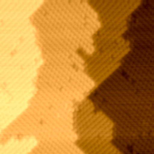
Standing wave on Cu (111) surface by USM-1300S VTI
 Yukio Hasegawa group
Univ. of Tokyo, Solid State Physics
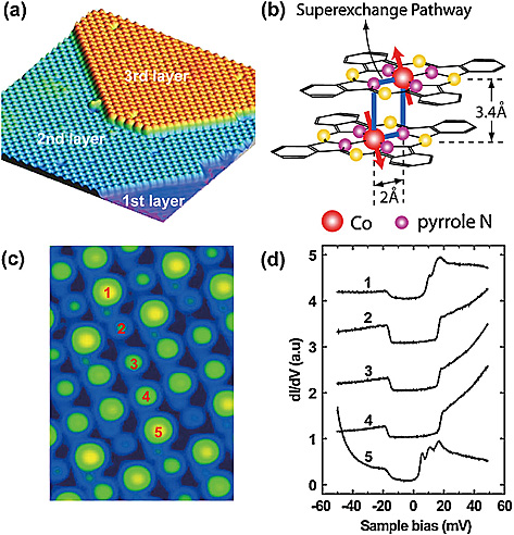
CoPc多層膜のSTM像とspin-flip IETS

(a)-(d): CoPc多層膜のSTM像とspin-flip IETS
観察温度 0.4K 磁場 1.5T (USM1300-3He)
Prof. Qi Kun Xue
Tsinghua University
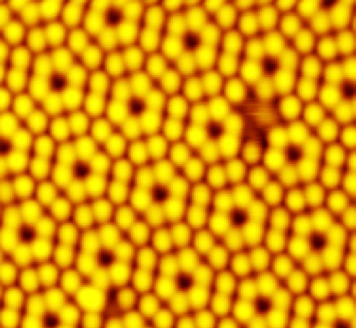
Si (111) 上のPbの√7×√3超構造のSTM像
Si (111) 上のPbの√7×√3超構造のSTM像
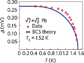
上記表面の超低温下での超伝導ギャップの温度依存性
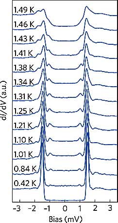
超伝導ギャップ幅の外部磁場強度依存性
Prof. Qi Kun Xue
Tsinghua University
USM1400
STM Topographic Image of Si (111) surface
Temperature: 83K
Scan area: 21.72nm × 21.72nm
Sample bias: 1.8V
Tunnel current: 0.54nA
Yuko Yamamoto
Unisoku Co., Ltd.
STM Topographic Image of Si (100) surface
Temperature: 83K
Scan area: 15.5nm × 4.3nm
Sample bias: 1.2V
Tunnel current: 1.0nA
Yuko Yamamoto
Unisoku Co., Ltd.
STM Topographic Image of Si (100) surface
Sample: Si (100)
Temperature: 83K
Scan area: 28.4nm × 28.4nm
Sample bias: -2V
Tunnel current: 0.2nA
Yuko Yamamoto
Unisoku Co., Ltd.
STM Topographic Image of Si (100) surface
Temperature: 83K
Scan area: 28.4nm × 28.4nm
Sample bias: 2V
Tunnel current: 0.2nA
USM1400-4P
4 point measurement
 Unisoku Co., Ltd.
STM image on HOPG at 6.5K
 Unisoku Co., Ltd.
Resistance of micro structure
 Unisoku Co., Ltd.
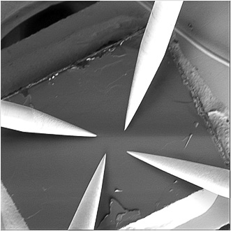
超高真空4プローブ表面電気特性測定装置 UMP1000-4P
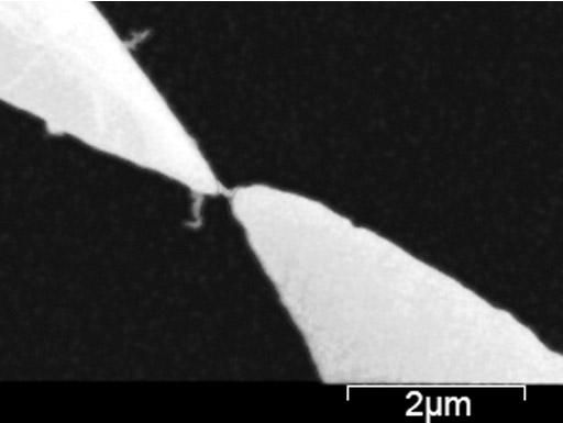
Four probes over carbon nanotube
Four-terminal Resistance measurement on Carbon Nanotube
Probe distance: <10μm
Prof. Sumiyama
Nagoya Institure of Technology
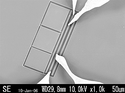
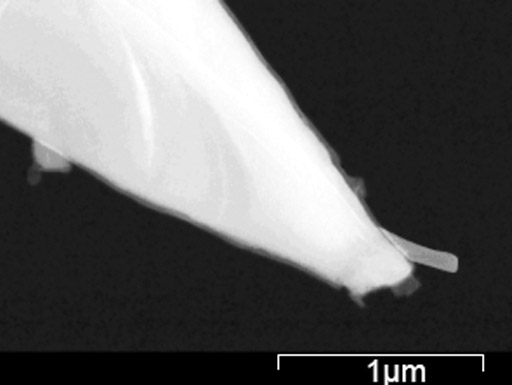
SEM Image of 4 Probes bellow 10K
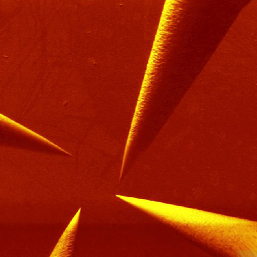
Scan area: 1mm × 1mm
Temprature: 6.5K
Yutaka Miyatake
Unisoku Co., Ltd.
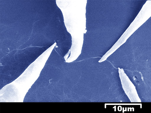
SEM Image of 4 Probes bellow 10K
Scan area: 15μm
Temprature: 6.5K
Yutaka Miyatake
Unisoku Co., Ltd.
Cutting CNT by 2 probes
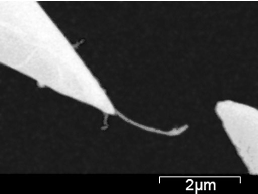
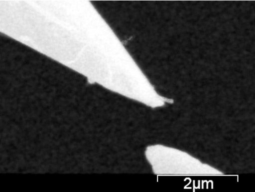
Applying a voltage across the probes
M.Yoshimura, Ueda Lab.,
Toyota Technological Institute
高真空STM 特注品
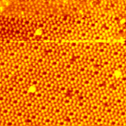
STM image of Mn Porpyrin molecules on Au (111)
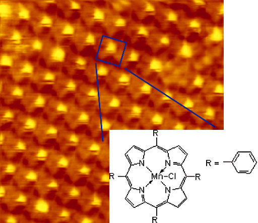
scan size: 10nm × 10nm 1.2V 10pA Unisoku Co., Ltd.
STM image of Au (111) herringbone structure
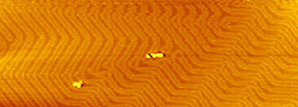
scan size: 180nm × 90nm Unisoku Co., Ltd.
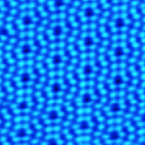
STM atomic image of Si (111) 7 × 7 structure
scan size: 12.8nm × 5.1nm
Dr. HANAGURI
in Magnetic Materials Laboratory, RIKEN
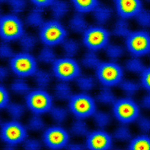
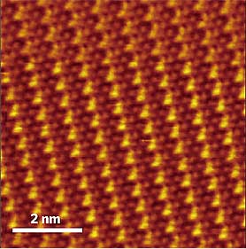
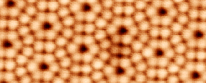
STM atomic image of √3 × √3-Ag structure on Si (111)
scan size 12nm × 12nm -0.4V 0.7nA Unisoku Co., Ltd.
超高真空AFM 特注品
AFM Topographic Image of Si (111) surface
div: Si (111) 7 × 7 by NC-AFM
Scan size: 13nm × 13nm
Cantilever: Piezo Resistive type (made by SII)
Frequency shift: -33Hz
Ichiro Shiraki
NIMS, Miki group